
Difference Between IC Substrate and PCB
A critical component in modern electronics, an integrated circuit substrate serves as the primary connection between a printed circuit board and the IC chip. The IC substrate does this through a network of conductive traces and holes, which are made possible by the use of different technologies. Understanding these technologies and the manufacturing process of IC substrate can help you make the right decision when it comes to a specific IC substrate for your project.
The IC substrate is used in various electronic products such as smartphones, tablets, and wearables. It can also be found in industrial control systems and power supplies. There are many benefits of using a PCB that contains an integrated circuit substrate, including increased functionality, lower cost, and improved reliability. However, the IC substrate manufacturing process is complex and requires advanced technology to produce high-quality results.
Unlike PCBs, which are used to manufacture circuit connections, ic substrate contain the conductive traces that connect the IC chip and the printed circuit board. They have a number of important characteristics that make them different from standard PCBs, such as their ability to handle higher circuit density and provide more accurate signal transmission. In addition, they are highly reusable and require less soldering to assemble.
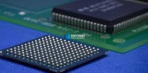
What is the Difference Between IC Substrate and PCB?
To ensure the integrity of the IC substrate, manufacturers must use the correct materials. This is because a faulty substrate can lead to a poor circuit design and poor performance, which can affect the end-user experience of the product. Moreover, a faulty substrate can also be expensive to repair.
It is also crucial that the IC substrate has the correct thickness and insulating properties. This is because it needs to be strong enough to support the IC chip and the other components on the PCB. It also needs to be lightweight and have good heat dissipation properties. In addition, the substrate must be able to provide good electrical conductivity and high levels of precision.
The IC substrate manufacturing process can be divided into three stages: copper patterning, copper plating, and etching. These steps are crucial in the development of an IC substrate, and each one correlates to diverse technological aspects, such as copper plating and patterning technology, circuit and control compensation technology, and fine-line fabrication technology.
As the demand for IC substrates rises, it is becoming more important for designers and engineers to understand the technology involved in the manufacturing process. This will help them select the best IC substrate for their project and achieve optimal performance. In order to do so, it is vital that they understand the unique attributes and characteristics of each type of IC substrate.
Some of the most common types of IC substrate include FR-4, HASL, and mSAP. Each of these has its own advantages and disadvantages. FR-4 has lower CTE (coefficient of thermal expansion) than other substrates, which makes it a good choice for high-speed traces. It is also durable and has a good solderability. However, it is important to note that FR-4 has some limitations, such as low dielectric constant and limited stack-up.


