
HDI PCB Improves Signal Integrity
The growing trend towards smaller electronics devices calls for advanced circuit boards that can deliver high performance in a small package. Using HDI technology, PCB designers can shrink components and improve signal integrity while keeping overall board size and costs down.
HDI PCBs are typically found in electronic devices that demand excellent performance while conserving space, such as mobile /cellular phones, touch-screen devices, laptop computers, digital cameras and 4/5G network communications. Military applications such as avionics and smart munitions also use HDI PCBs. These advanced boards have lower copper traces, tighter trace spacing and narrow annular rings, higher layer counts, smaller vias, and specialty materials to increase component density, improve performance, and minimize cost.
A typical 2-4-2 stacked hdi pcb construction is manufactured in the same way as a standard multilayer board, with layers 2 and 7 being laser drilled to form microvias before lamination. The inner layers are etched, the blind microvias are filled with conductive paste, and the outer layers are laminated to complete the structure.
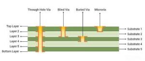
How HDI PCB Improves Signal Integrity
Because of the increased component density and complex interconnections in an HDI PCB, it is essential to ensure proper routing techniques to reduce signal degradation and electromagnetic interference (EMI). Impedance mismatch, crosstalk, and other factors can cause errors and signal quality issues that negatively impact device functionality and performance. Proper design practices can improve signal integrity in an HDI PCB, including via stitching to connect ground planes, effective decoupling techniques, and compliance with applicable EMI/EMC standards.
Various factors can cause impedance mismatch in an HDI PCB, ranging from varying trace widths to excessive spacing between adjacent traces. These factors can lead to signal reflections, which decrease the effective bandwidth of a signal, and increase transmission delays and skew, resulting in poor system performance. To avoid these issues, it is important to select a PCB material with a low dielectric constant for reduced signal distortion and propagation delay, as well as a high thermal conductivity to eliminate power loss and prevent hot spots that can interfere with signal performance.
Stitching techniques to connect the ground planes across multiple layers of an HDI PCB can provide a low-impedance return path for signals and reduce signal bounce. Adding signal transition vias between different layers can also improve signal transmission and reduce interference and crosstalk. Finally, utilizing signal transition vias to avoid signal overlapping between layers can help achieve impedance matching and minimize signal degradation.
High-speed signal integrity in HDI PCBs requires a careful design process, specialized materials and fabrication processes, and rigorous testing and inspection to ensure optimum performance. To meet these demands, engineers must optimize signal transmission and improve impedance matching by reducing via inductance, using back-drilling techniques for through-hole vias, and considering buried or blind via structures. In addition, they must use a stable power distribution network (PDN) to stabilize power fluctuations and suppress noise, and employ decoupling techniques to mitigate high-frequency signal interference. Finally, a comprehensive test and simulation program is necessary to verify that the final product meets impedance specifications.


